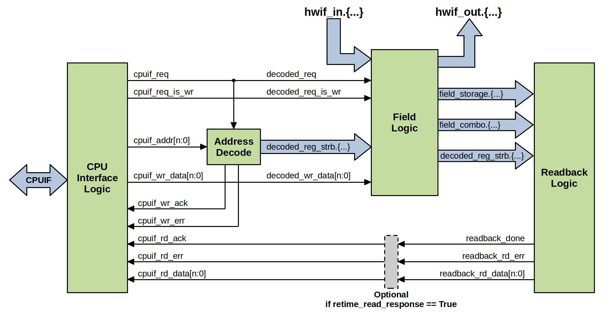
Register Block Architecture#
The generated register block RTL is organized into several sections. Each section is automatically generated based on the source register model and is rendered into the output register block SystemVerilog RTL.
Although it is not completely necessary to know the inner workings of the generated RTL, it can be helpful to understand the implications of various exporter configuration options.
CPU Interface#
The CPU interface logic layer provides an abstraction between the application-specific bus protocol and the internal register file logic. This logic layer normalizes external CPU read & write transactions into a common Internal CPUIF Protocol that is used to interact with the register file.
Address Decode#
A common address decode operation is generated which computes individual access strobes for each software-accessible register in the design. This operation is performed completely combinationally.
Field Logic#
This layer of the register block implements the storage elements and state-change logic for every field in the design. Field state is updated based on address decode strobes from software read/write actions, as well as events from the hardware interface input struct. This section also assigns any hardware interface outputs.
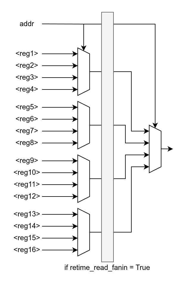
Readback#
The readback layer aggregates and MUXes all readable registers into a single read response.
For designs with a large number of software-readable registers, an optional fanin re-timing stage can be enabled. This stage is automatically inserted at a balanced point in the read-data reduction so that fanin and logic-levels are optimally reduced.
A second optional read response retiming register can be enabled in-line with the path back to the CPU interface layer. This can be useful if the CPU interface protocol used has a fully combinational response path, and the design’s complexity requires this path to be retimed further.